 | –≠–ª–µ–∫—Ç—Ä–æ–Ω–Ω—ã–π –∫–æ–º–ø–æ–Ω–µ–Ω—Ç: UPG133G | –°–∫–∞—á–∞—Ç—å:  PDF PDF  ZIP ZIP |
GaAs INTEGRATED CIRCUIT
P
P
P
P
PG138GV
L-BAND SPDT SWITCH
1996
©
Document No. P13058EJ2V0DS00 (2nd edition)
(Previous No. P11508EJ1V0DS00)
Date Published December 1997 N CP(K)
Printed in Japan
DATA SHEET
DESCRIPTION
The
P
PG138GV is L-Band SPDT (Single Pole Double Throw) GaAs FET switch which was developed for digital
mobile communication system.
It housed in an very small 8-pin SSOP that is smaller than usual 8-pin SOP and easy to install and contributes to
miniaturizing the system.
FEATURES
∑ Maximum transmission power : +35 dBm min. (@ V
CONT
=
5 V/0 V:
P
PG138GV
)
+34 dBm typ. (@ V
CONT
=
3 V/0 V:
P
PG138GV)
∑ Low insertion loss
: 0.55 dB typ. (@ 1 GHz)
0.65 dB typ. (@ 2 GHz)
APPLICATION
∑ Digital Cellular : GSM, PDC, PCN etc.
∑ PHS Base Station, PCS etc.
ORDERING INFORMATION
PART NUMBER
PACKAGE
PACKING FORM
P
PG138GV-E1
8-pin plastic SSOP (175 mil)
Carrier tape width 12 mm Qty 2 kp/Reel.
ABSOLUTE MAXIMUM RATINGS (T
A
= 25 ∞C)
PARAMETERS
SYMBOL
RATINGS
UNIT
Control Voltage 1, 2
V
CONT1, 2
6.0 to +0.6
V
Input Power (V
CONT
=
5 V)
P
in
+36
dBm
Input Power (V
CONT
=
3 V)
P
in
+34
dBm
Total Power Dissipation
P
tot
0.7
W
Operating Temperature
T
opt
50 to +80
∞C
Storage Temperature
T
stg
65 to +150
∞C
2
P
P
P
P
PG138GV
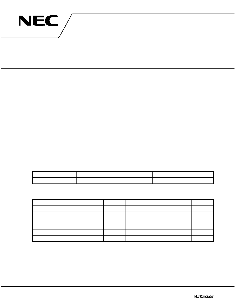
PIN CONNECTION DIAGRAM (Top View)
1
2
3
4
8
7
6
5
1. V
CONT2
2. OUT2
3. GND
4. GND
5. IN
6. GND
7. OUT1
8. V
CONT1
G138
SPDT SWITCH IC SERIES PRODUCTS
PART
NUMBER
PIN (1 dB)
(dBm)
LINS (dB)
ISL (dB)
VCONT (V)
PACKAGE
APPLICATIONS
P
PG130G
+34
0.5 @ 1 G
32 @ 1 G
5/0
PDC, IS-54, PHS
P
PG131G
+30
0.6 @ 2 G
23 @ 2 G
4/0
PHS, DIVERSITY
P
PG132G
+30
0.6 @ 2 G
22 @ 2 G
+3/0
PHS, DIVERSITY
P
PG133G
+25
0.6 @ 2 G
20 @ 2 G
3/0
DIVERSITY, VCO
P
PG137GV
+34
0.55 @ 1 G
25 @ 2 G
+3/0
PDC, GSM, IS-136
P
PG138GV
+34
+38
0.55 @ 1 G
30 @ 1 G
3/0
5/0
PDC, GSM, IS-136
Remark
As for detail information of series products, please refer to each data sheet.
8 pins SSOP
(175 mil)
3
P
P
P
P
PG138GV
[
P
P
P
P
PG138GV]
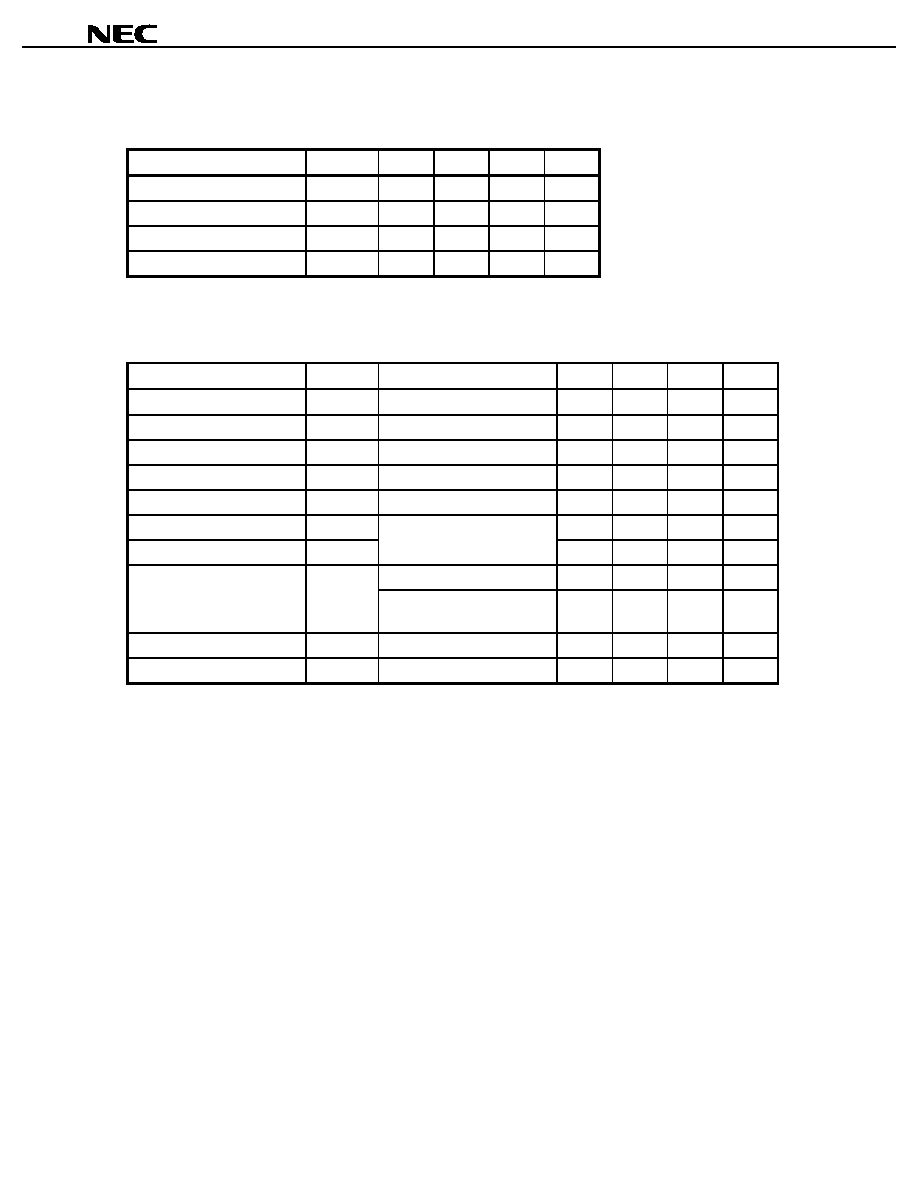
RECOMMENDED OPERATION CONDITIONS
PARAMETER
SYMBOL
MIN.
TYP.
MAX.
UNIT
Control Voltage (ON)
V
CONT
0.2
0
+0.2
V
Control Voltage (OFF)
V
CONT
5.3
3.0
2.7
V
Input Power (V
CONT
=
5 V)
P
in
+35
dBm
Input Power (V
CONT
=
3 V)
P
in
+33
dBm
ELECTRICAL CHARACTERISTICS
(UNLESS OTHERWISE SPECIFIED T
A
= 25
q
q
q
q
C, V
CONT
=
3 V/0 V, f = 100 MHz to 1 GHz)
CHARACTERISTICS
SYMBOL
TEST CONDITION
MIN.
TYP.
MAX.
UNIT
Insertion Loss 1
L
INS1
0.55
0.75
dB
Insertion Loss 2
L
INS2
f = 2.0 GHz
0.65
0.90
dB
Insertion Loss 3
L
INS3
f = 2.5 GHz
0.8
Note 1
dB
Isolation 1
I
SL1
25
30
dB
Isolation 2
I
SL2
f = 2.0 GHz
18
20
dB
Input Return Loss
RL
in
f = 100 M to 2 GHz
11
dB
Output Return Loss
RL
out
11
dB
Input Power at 1 dB
P
in
(1 dB)
f = 500 M to 2 GHz
+32
+34
dBm
Compression Point
Note 2
f = 500 M to 2 GHz,
V
CONT
=
5 V/0 V
+34
+38
dBm
Switching Speed
t
SW
10
ns
Control Current
I
CONT
V
CONT
=
5 V/0 V
5
P
A
Notes 1. Characteristic for reference at 2.0 to 2.5 GHz.
2. P
in
(1 dB) is measured the input power level when the insertion loss increase more 1 dB than that of
linear range.
All other characteristics are measured in linear range.
NOTE ON CORRECT USE
∑
Insertion loss and isolation of the IN-OUT2 is better than that of IN-OUT1, because No. 7 pin (OUT1) is placed to
same side of No. 5 pin (IN).
∑
The distance between IC's GND pins and ground pattarn of substrate should be as shorter as possible to avoid
parasitic parameters.
4
P
P
P
P
PG138GV
[
P
P
P
P
PG138GV]
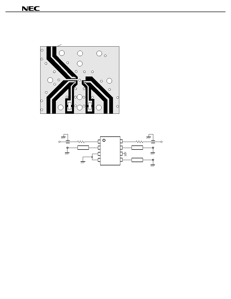
TEST BOARD
R
R
NEC
G130/131
0.4 mm
thickness
teflon glass
R = 50
Using the same board that of PG130/131G
IN
0.9 mm width
OUT1
V
CONT1
V
CONT2
OUT2
µ
TEST CIRCUIT
1
2
3
4
8
7
6
5
50
50
V
CONT2
= 0 V/≠3 V
OUT2
1000 pF
Z
O
= 50
1000 pF
V
CONT1
= ≠3 V/0 V
OUT1
IN
Z
O
= 50
Z
O
= 50
5
P
P
P
P
PG138GV
[
P
P
P
P
PG138GV]
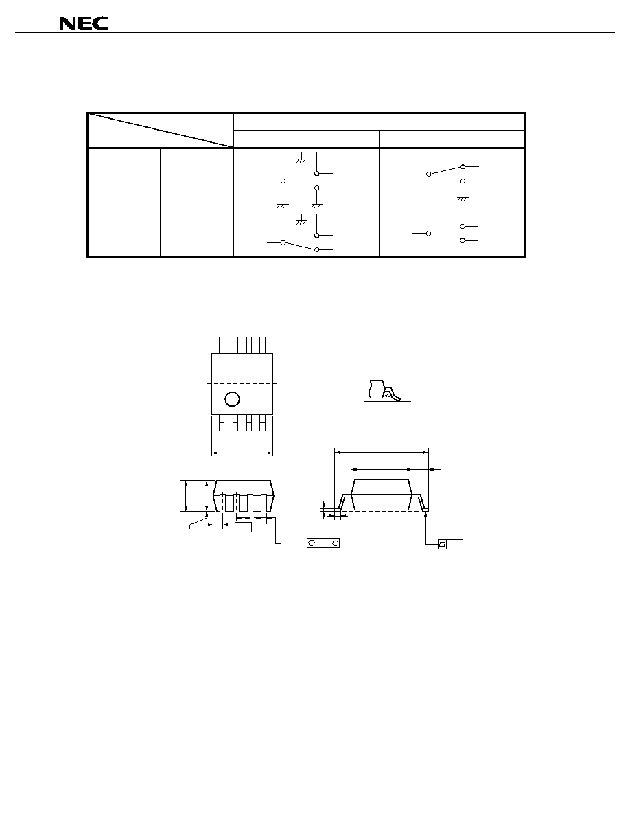
TRUTH TABLE OF SWITCHING BY CONDITION OF CONTROL VOLTAGE
V
CONT1
0 V
3 V
V
CONT2
0 V
OUT1
OUT2
IN
OUT1
OUT2
IN
3 V
OUT1
OUT2
IN
OUT1
OUT2
IN
PACKGE DIMENSIONS
8-PIN PLASTIC SHRINK SOP (175 mil) (Unit mm)
8
5
1
4
3.0 MAX
0.15
0.87 ± 0.2
4.94 ± 0.2
3.2 ± 0.1
0.15
+0.10 ≠0.05
0.5 ± 0.2
3∞
+7∞ ≠3∞
0.575 MAX
0.1 ± 0.1
1.8 MAX
1.5 ± 0.1
0.10
M
0.3
+0.10
≠0.05
0.65
Detail of lead end